The AI Memory Wall: Why HBM4 Matters More Than the Next GPU Generation
The narrative around AI hardware has always centered on compute: petaflops, TFLOPS, the number of tensor cores, the transistor count. But the frontier of AI model performance in 2025-2026 is increasingly constrained not by how fast GPUs can compute, but by how fast they can read data. The bottleneck is memory bandwidth — and the industry's answer is HBM4.
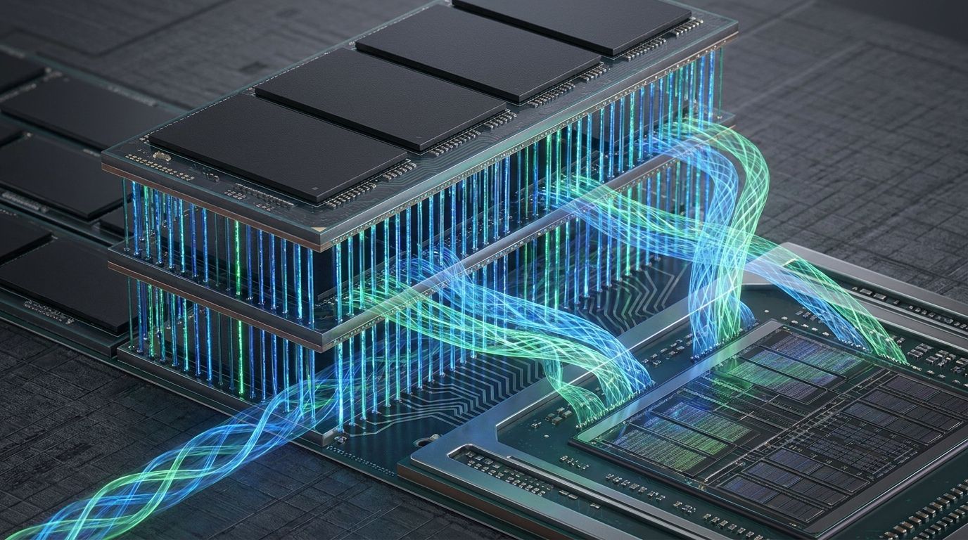
High Bandwidth Memory (HBM) is the stacked DRAM technology that sits on the same package as GPU silicon, connected by thousands of short, wide electrical connections called through-silicon vias (TSVs). Each "stack" is multiple DRAM dies bonded vertically, with the interface between them far wider — and therefore far faster — than the PCB traces connecting conventional off-package memory. HBM3e, shipping on Nvidia's H200 and AMD's Instinct MI325X, delivers up to 4.8 terabytes per second (TB/s) of memory bandwidth. HBM4, in production at SK Hynix and Samsung and shipping in 2025-2026, pushes that past 6 TB/s per stack — with die-to-die bandwidth increasing substantially through a new 2048-bit interface.
Why Bandwidth Became the Constraint
Modern transformer models are memory-bandwidth-bound during inference in a way that was not true during training. Here's why: training processes large batches of data through the model simultaneously, which means the GPU's compute units stay busy. But inference — responding to a single user query — involves much smaller batch sizes, often batch size 1. At batch size 1, the GPU spends most of its time reading model weights from memory and relatively little time doing arithmetic on them. The ratio of arithmetic operations to memory reads, called arithmetic intensity, is low.
For a model like Llama 3 70B at float16 precision, you need to move roughly 140 GB of weights from memory to compute for every forward pass. At H100 SXM5 bandwidth of 3.35 TB/s, that takes about 42 milliseconds per token — before any actual computation. The GPU's 2,000 TFLOPS of theoretical compute sits mostly idle, starved for data. Doubling compute without doubling bandwidth changes almost nothing for single-user inference.
This is the memory wall: a regime where raw compute improvements produce diminishing returns because the system cannot move data fast enough to keep the processors fed.
What HBM4 Actually Changes
HBM4 does not just add bandwidth — it changes the architecture of how memory is attached to compute. HBM3e uses a 1024-bit interface per stack; HBM4 doubles this to 2048 bits. Combined with higher clock speeds, this roughly doubles per-stack bandwidth. More importantly, the new standard enables base-die logic — a compute layer inside the memory stack itself, adjacent to the data — which allows simple operations to be performed without moving data to the GPU at all.
Nvidia's Blackwell B200 ships with HBM3e, delivering 8 TB/s aggregate across its five stacks. The successor, Vera Rubin, is expected to use HBM4 and target 15+ TB/s. For inference workloads, this is a more meaningful improvement than doubling FP8 compute. AMD's Instinct MI350X also targets HBM3e scaling, with MI400 planned around HBM4.
The bandwidth improvement affects more than inference latency. Larger effective batch sizes become possible without memory thrashing, which improves GPU utilization during inference and makes continuous batching strategies (the technique used by vLLM to serve hundreds of users simultaneously on a single GPU) more efficient.
The Capacity Problem
Bandwidth is only part of the memory challenge. Model size is growing too, and fitting a model in memory is a prerequisite for serving it. GPT-4-class models are widely estimated at 1-8 trillion parameters; even at 4-bit quantization, a 1T parameter model requires 500 GB of memory. Current HBM3e configurations on H100 systems top out at 80 GB per GPU, requiring clusters of 8-16 GPUs even for quantized models.
HBM4 addresses this partly through improved density. SK Hynix's 12-high HBM4 stacks can achieve 48 GB per stack, versus 24 GB in current HBM3e. Combined with six stacks per GPU, this could bring per-GPU memory to 288 GB — enough to serve mid-size frontier models on a single chip.
For training, the math is different: gradient storage and optimizer states multiply memory requirements by 12-16x per parameter. A 7B parameter model in float32 with AdamW optimizer states requires roughly 112 GB — the entire memory of a single H100 node. Distributed training across hundreds of GPUs is standard practice, but each communication step introduces latency proportional to model size.
The Supply Chain Complication
HBM is manufactured by three companies: SK Hynix, Samsung, and Micron. Hynix is the technology leader and Nvidia's primary supplier for HBM3e. Samsung has struggled with HBM3e yield issues, costing it Nvidia qualification. Micron's HBM3e is in production and shipping to AMD.
The concentration risk is real. Nvidia consumes a large portion of global HBM output, and shortages of HBM capacity have contributed to GPU supply constraints that are structurally separate from GPU fabrication capacity at TSMC. Building more GPU logic chips does not help if there is not enough HBM to attach to them. Analysts estimate HBM supply remains constrained through 2026, with pricing elevated relative to standard DRAM.
HBM4 production requires even tighter integration between memory manufacturer and chip designer — the new base-die compute capability requires joint design of the memory stack and the GPU package. This deepens the partnership requirements between Nvidia and SK Hynix, raising barriers to new entrants.
Beyond GPUs: The Compute-Near-Memory Future
The longer-term trajectory points toward a more fundamental architectural shift: processing-in-memory (PIM) and near-memory computing, where compute elements move closer to where data lives rather than the other way around. HBM4's base-die logic is an early step in this direction.
Several startups — Untether AI, Mythic, and Axelera among them — are building inference chips that place compute directly adjacent to dense memory arrays, eliminating the bandwidth wall by design. These have not displaced GPU-based inference at scale, but they demonstrate where the architectural pressure leads. The memory wall is not a temporary problem to be patched with faster buses — it is a consequence of the von Neumann architecture's separation of compute and storage, and solving it requires rethinking that separation.
For the next two to three years, HBM4 is the practical answer. But the companies that win the next phase of AI hardware may not be the ones with the fastest compute — they will be the ones that figure out how to eliminate the memory bottleneck by design.