The Chiplet Revolution: How AMD, Intel, and TSMC Are Building CPUs Like LEGO Bricks
The transistor density curve that drove 50 years of processor performance gains is flattening. Moving to a smaller process node — from 7nm to 5nm to 3nm — gets more expensive and yields fewer benefits each generation. The semiconductor industry's answer is not to wait for better lithography. It's to rethink what a chip is.
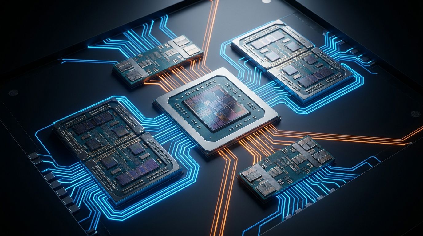
The chiplet approach breaks a processor into multiple smaller dies, each manufactured on the process node best suited to its function, and connects them using a high-bandwidth, low-latency interconnect on a shared package. The result behaves like a single chip to software but is physically a collection of specialized tiles — a CPU compute tile here, an I/O tile there, a memory controller over there.
Why Monolithic Dies Hit a Wall
The economics of semiconductor manufacturing are brutal. Defects are randomly distributed across a wafer, and larger dies have a higher probability of containing at least one defect. A 500mm² monolithic die has roughly 3x worse yield than two 250mm² dies that together cover the same area. At leading-edge nodes — where wafer costs can exceed $20,000 — this yield penalty directly translates to unit cost.
There's also the cross-node optimization problem. Memory controllers, I/O interfaces, and analog circuits do not benefit from the smallest process nodes the way logic does. Running everything at 3nm wastes money on components that perform perfectly well at 12nm or even 22nm. Chiplets let engineers use the right node for each function.
AMD's Bet That Changed the Industry
AMD's first commercial chiplet product was the Zen 2 generation Ryzen 3000 CPUs in 2019. The design split the processor into compute dies (built on TSMC's 7nm node) and an I/O die (built on GlobalFoundries' 12nm node). The compute dies contained the CPU cores and L3 cache; the I/O die contained the memory controller, PCIe lanes, and USB/SATA interfaces.
The commercial impact was immediate. AMD could now scale core count by adding compute dies without redesigning the entire chip, while keeping the expensive 7nm real estate focused on the transistors that most benefit from it. The Ryzen Threadripper 3990X, released the same year, used this approach to deliver 64 cores — previously impossible on a single affordable die.
With the Ryzen 7000 series and EPYC Genoa server chips, AMD pushed further. The 3D V-Cache variant stacks an additional 64MB of L3 cache directly on top of the compute die using through-silicon vias, treating the cache itself as a chiplet bonded vertically. Benchmarks showed 10–30% performance gains in cache-sensitive workloads like gaming and scientific simulations — not from better transistors, but from a better physical arrangement of them.
Intel's Response: Tiles and EMIB
Intel was slower to embrace chiplets publicly — the company had built its reputation on monolithic integration — but its 2021 Alder Lake hybrid architecture (mixing performance and efficiency cores) signaled a shift. By 2023, Intel Meteor Lake was the company's first fully tile-based consumer processor, decomposing the chip into a CPU tile, GPU tile, SoC tile, and I/O extender tile, each on a different process node.
Intel's key interconnect technology is EMIB (Embedded Multi-die Interconnect Bridge), a small piece of silicon embedded in the package substrate that provides a dense, high-bandwidth connection between adjacent dies without requiring an expensive interposer across the entire package. For the high-bandwidth connections needed between CPU and GPU tiles in products like the Ponte Vecchio data center GPU, Intel uses a more advanced variant called Foveros Direct, which allows face-to-face die stacking with direct copper-to-copper bonding at 10µm pitch.
TSMC's CoWoS and the AI Packaging Race
The AI chip boom has made TSMC's advanced packaging business as strategically important as its leading-edge logic fabs. CoWoS (Chip-on-Wafer-on-Substrate) is the packaging technology behind Nvidia's H100 and H200 GPUs — it places the GPU die and HBM memory dies side-by-side on a silicon interposer, enabling the 3.35TB/s memory bandwidth that makes large language model training practical.
Nvidia's Blackwell B200 pushes CoWoS further: two GPU dies connected by a 10TB/s NVLink chip-to-chip interconnect form a single logical GPU with 208 billion transistors. From software's perspective, it's one device. Physically, it's a carefully engineered multi-die assembly that no single lithography machine could pattern.
The CoWoS supply constraint in 2024–2025 was one of the primary bottlenecks in the AI chip shortage. TSMC's advanced packaging capacity was months behind demand, and lead times for CoWoS substrates stretched to 52 weeks at peak. TSMC has since expanded packaging capacity significantly, but the episode illustrated how packaging — once considered a commodity — has become a first-class competitive variable.
The Interconnect Problem
The open question in chiplet design is interconnect standardization. AMD, Intel, and TSMC each use proprietary die-to-die interfaces. For a chip manufacturer to buy compute chiplets from one vendor and I/O chiplets from another, both must speak the same protocol at the physical layer.
The Universal Chiplet Interconnect Express (UCIe) consortium, launched in 2022 with founding members including Intel, AMD, Arm, TSMC, and Samsung, is working to solve this. UCIe defines a standard physical layer and protocol for die-to-die communication, targeting bandwidths up to 28Gbps per wire at sub-2pJ/bit energy. Adoption is gradual: UCIe 1.1 was published in 2023, and the first products using it began sampling in 2025.
If UCIe succeeds, it enables a chiplet marketplace: buy CPU cores from AMD, a neural processing unit from Qualcomm, memory controllers from a specialist, and assemble them into a custom SoC — a model that would radically change both the economics and competitive dynamics of chip design. The precedent from the PCIe and USB standards suggests standardization will eventually happen. The question is how long the major players resist standardization to protect their packaging moats.
What This Means for the Next Five Years
Chiplets are no longer experimental — they're the mainstream architecture for any chip above a certain complexity threshold. AMD's entire datacenter lineup, Nvidia's flagship GPUs, Intel's Meteor and Arrow Lake consumer processors, Apple's M-Ultra and M4 Max chips (which combine two dies with Apple's Ultra Fusion interconnect), and virtually every high-end networking ASIC now use some form of multi-die assembly.
The practical consequence for buyers is that the node number on the spec sheet tells only part of the story. A "3nm" CPU that uses a 12nm I/O die alongside it is not entirely 3nm — but it may outperform a monolithic 3nm chip because the overall die composition is better optimized. Understanding chiplet architecture is increasingly necessary to evaluate processor performance claims accurately.